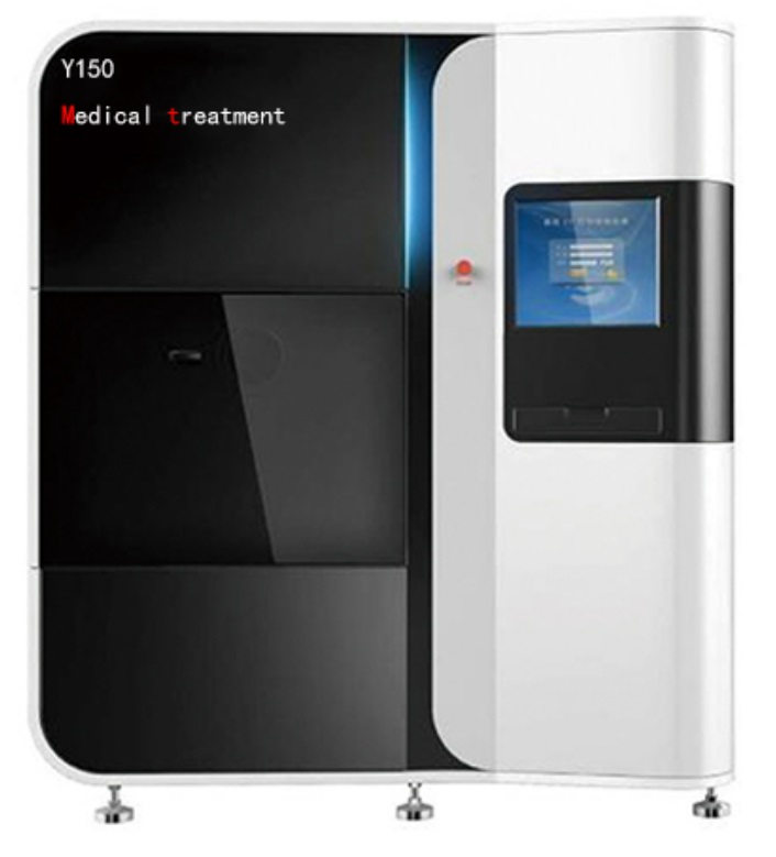
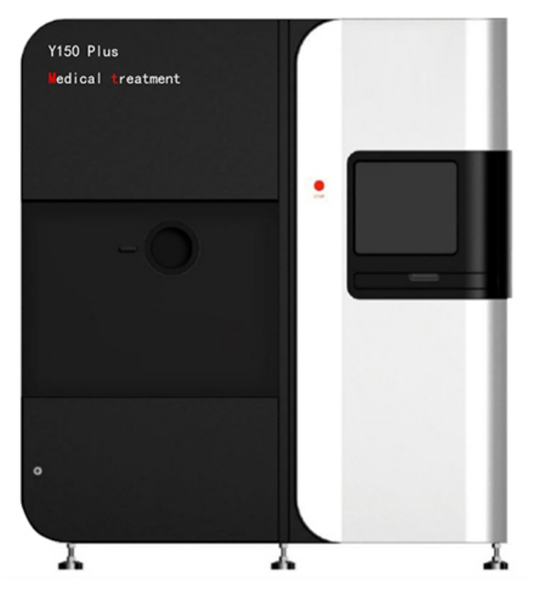
PBF-SEBM 3D Printing System (SEBM-Y150 / Y150Plus)
Target groups:
The users who make the complex metal parts either in small batch production or for prototypes with powder bed fusion technology – selective electron beam melting process, specially for production of implants.
Application:
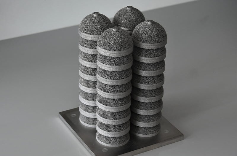
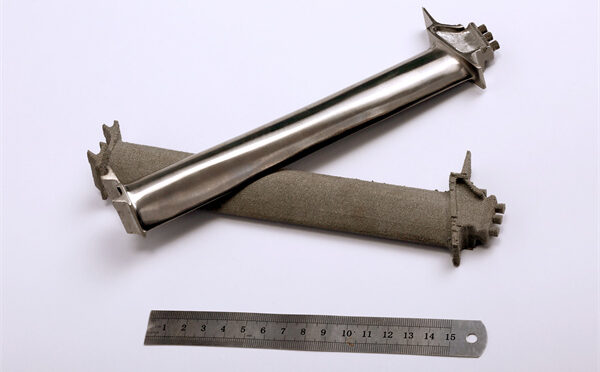
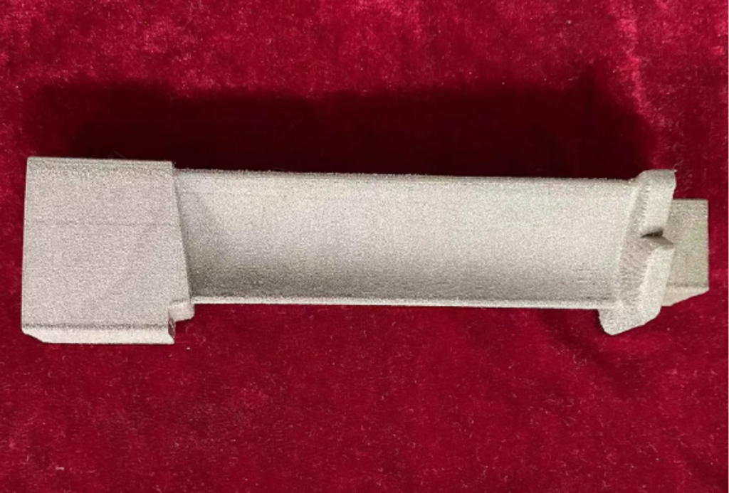
Production of complex/customized metal parts, such as:
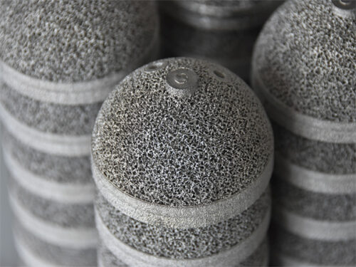
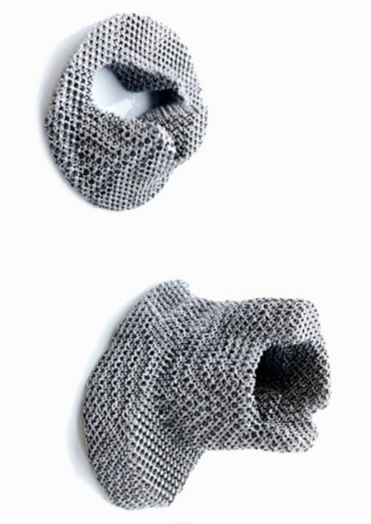
Orthopedic implants
TiAl blades / components
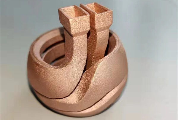
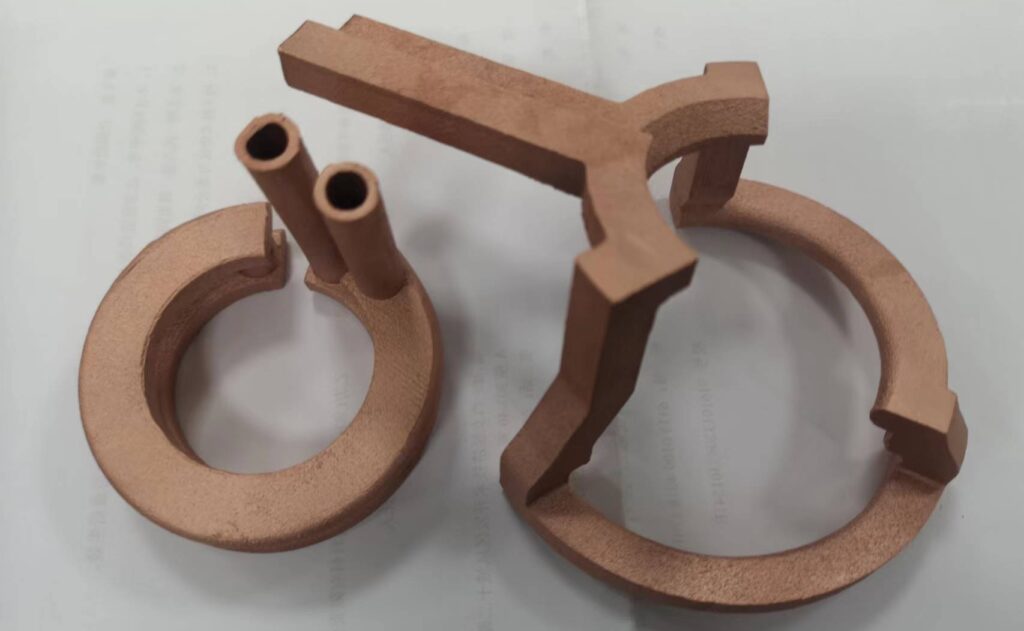
Copper coils for induction hardening
Other metal components
Main Advantage
Build size: 170mm x 170mm x 180mm
The minimum beam diameter is less than 100μm for SEBM-Y150Plus and 300μm for SEBM-Y150.
Higher productivity thanks to higher energy density, lower reflectivity and strong penetration abilities to materials of electron beam and stacking capabilities;
Better product performance thanks to forming in a controllable vacuum environment and higher pre-heating (up to 1300℃) during printing;
Able to print the active and brittle metal powders (such as TiAl intermetallic compounds, pure copper, etc.) thanks to higher pre-heating temperature, higher energy density and vacuum environment, etc. (less internal stress and significantly reduces the risk of internal cracks);
No extra heat treatment during post-treatment is needed for some materials thanks to higher temperature pre-heating and heat-remaining of the whole powder bed during printing;
Easier post treatment thanks to the “fake sintering” capabilities during printing (no/less machining to remove the supports, normally, high-pressure compressed gas can be used to remove the excess powders which can be recycled);
Fully open source: customers can develop the process parameters according to their requirements (Materials, target part complexity, target part dimension tolerances, etc.).
Basic principle
Powder Bed Selective Electron Beam Melting process (SEBM) is an additive manufacturing technology that uses high-energy electron beams as energy source to manufacture metal components in a high vacuum environment by melting metal powders layer by layer.
The process is: The electron beam quickly scans, pre-heats and melts the pre-laid spherical metal powders on the substrate plate according to the planned path. After completing a layer of scanning and melting, the substrate plate descends to a certain height and a new powder layer is laid. The electron beam scans and melts again according to the planned path, …, so the process is repeated layer by layer like this, finally, the metal parts are manufactured completely from 2D to 3D.
Technical characteristics
Electron beam as heat source with high energy density, high absorbtion and conversion rate to the printed materails with strong penetration ability to have deeper molten pool and denser formed parts
Stacking production capabilities
Pre-heating temperature up to 1300℃ or more
Fake support (no/less supports are needed)
Lower cost materials
Forming in the vacuum environment
Main Technical Parameters
Max.build size
170×170×180 mm
Beam power
3 kW
Electron accelerating voltage
60 kV
Beam current
0~50 mA
Filament life
>60 h for SEBM-Y150 >500 h for SEBM-Y150Plus
Cathode type
Directly heated tungsten cathode
Min.beam diameter
≤300 μm for SEBM-Y150 ≤100 μm for SEBM-Y150Plus
Max. powder bed preheat temperature
1300 ℃
Ultimate vacuum
5×10⁻³ Pa
Build accuracy of components
±0.2 mm
External dimension
2000×1200×2150 mm3
Machine weight
1.5 t
CAD (interface)
STL
Control software
SEBM-ICS
Printable Materials
Titanium alloys (such as Ti6Al4V)
Refractory metals (such as pure Tungsten, Tantalum, Niobium, Molybdenum, etc.)
Titanium Aluminum alloys (Such as TiAl4822, etc.)
Copper alloys
Zirconium alloys
Nickel-base superalloys (Such as Inconel 718, Inconel 625, etc.)